Digitally controlled, dual channel power supply – part1
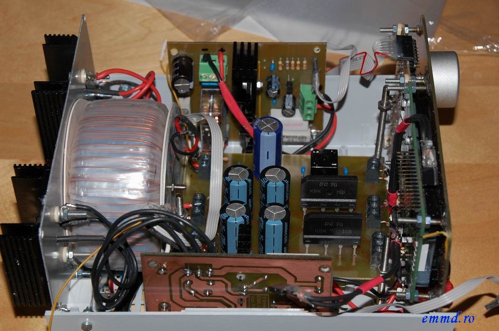
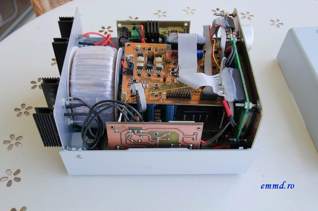
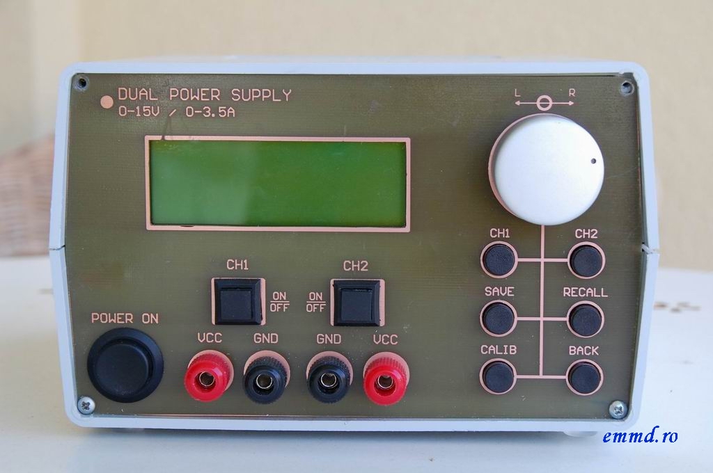
A project I created many years ago, a 2 channels, digitally controlled power supply. I built it to fit in a small plastic box 20 x 18 x 11 cm (L x W x H ). Each channel can provide 0…15 Volt output with up to 6 AMPs. I replaced the original front panel with a custom made (PCB design) to have all buttons, connectors and switches better highlighted. The back cover is the original one, but drilled to fit the power plug, a DB9 connector, the fuse and support for 2 high power transistors together with heatsinks. There is no dedicated power supply management chip. Everything is controlled by the main CPU, an ARM7 from NXP: LPC2103. I designed this device to have several nice features, easy to use and suitable also for lab usage.
Main characteristics:
- 2 channels, 0…15Volt, up to 6AMPs;
- each channel can be independently controlled: voltage + current limit + output ON/OFF;
- 6 preset positions: voltage + current limit: add/erase;
- self calibration feature;
- short-circuit protection;
- current overload protection;
- voltage output kept constant regardless of current consumption;
- possibility to control it over UART interface from PC (no application included, only the protocol);
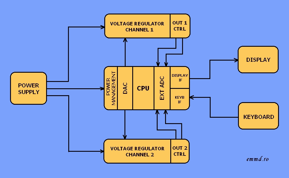
Here below a snapshot with block architecture:
In part 1 you’ll find details about the hardware design (schematic & PCB layout) + some pictures with the boards assembled. In part you can find details about the firmware functionality.
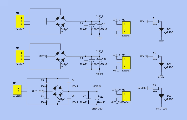
Main power supply: it contains 3 separate blocks, 2 for the analog voltage regulators + 1 for digital board. I used a toroidal transformer which came by default with 2 x 15Volt so I modified it for the 3rd 15V output. The consumption for digital part should be low, so I don’t expect it to overheat. 4700uF is the filtering on each channel + proper bridge rectifiers to support high currents (for analog channels).
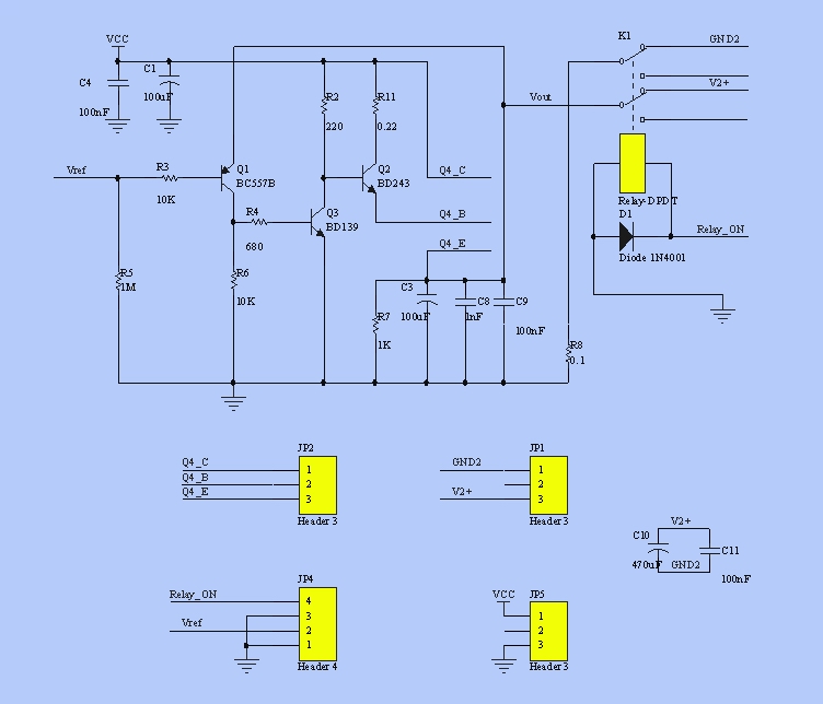
Analog voltage regulators: there are 2 identical voltage regulators, each of them is powered up by 22-24Volt. The voltage level is adjusted by Vref input, as following: *** When Vref decreases, the voltage across R3 gets higher so the current on Q1 base will raise. This, in turn, will raise the current on R6, hence the voltage across it will go up. Q3 will get more current on the base so C-E voltage will decrease (voltage across R2 will increase in the same time) => Q2 base will be driven low. In this way Q4 will be driven low too, decreasing the output voltage. How much? If we look at the schematic, we see that Q1 emitter is linked to output line, so once the output voltage decreases, it will decrease also the voltage across Q1, hence the voltage on R3 will go down until the equilibrium is met. *** When Vref increases, the mechanism goes in the opposite way: R3 voltage goes down => R6 voltage goes down => Q3 starts closing itself (Q3 C-E increases) => Q2 & Q4 base voltages are increased, hence output voltage will raise. This, in turn, will set Q1 emitter to a higher value raising the voltage across R3, untill, again, the equilibrium is met. R8 is a high power resistor, 0,1 Ohm, used to measure the current consumed at a certain moment. If we consider 6 AMPs the maximum current consumption, then 6 * 0,1 = 0,6 Volts should be the equivalent voltage measured. This signal is fetched to the external AD convertor on the digital board. GND2 is the real ground line connected to the user interface, GND signal being used only internally. The PCB still needs a wired connection (preferably on the top side) between Q2 base and Q3 collector. R2, R8 and R11 are 5W resistors.
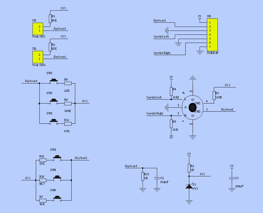
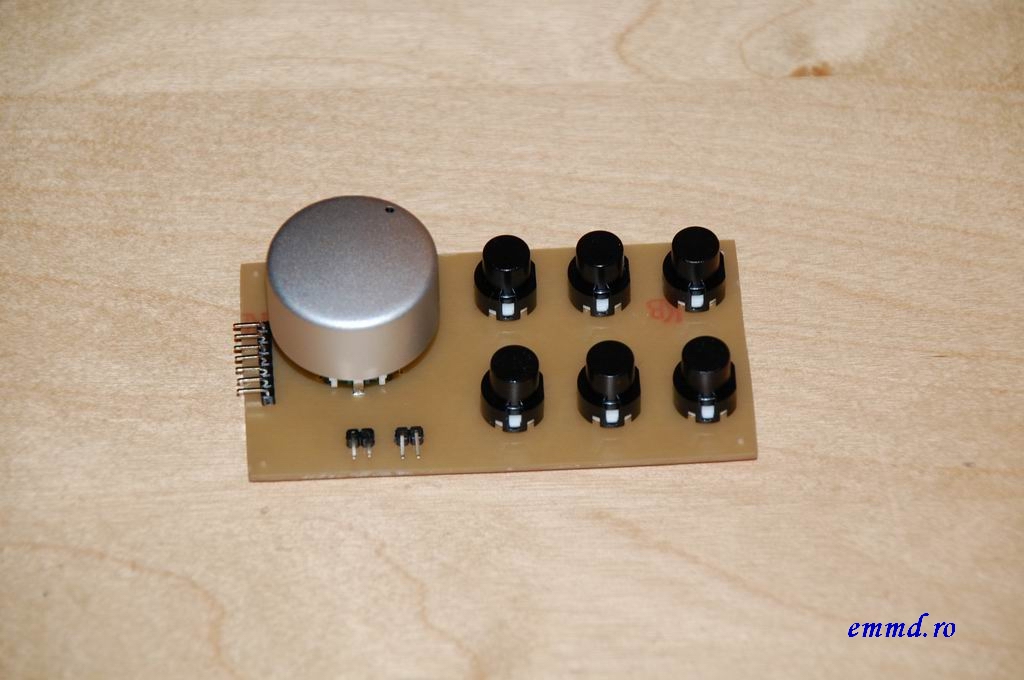
User interface: contains 6 buttons for the normal menu navigation & adjusting(SW1 to SW6) + 2 buttons for output control linked to JP1 & JP2 (1 button ON/OFF for each channel) + a rotary encoder from ALPS (STEC12E08) with push switch integrated. Apart of the encoder, all other switches enable some resistor dividers, setting a specific voltage on “Keyboard” line, which is connected to the internal AD converter. The encoder is not the best one, having lots of fake transitions, but with a good software algorithm can be read with good accuracy. It works in the following way: during rotation, the 2 outputs named “Joystick Left” & “Joystick Right” will toggle giving several states. These have to be decoded by software to get the proper rotating direction.
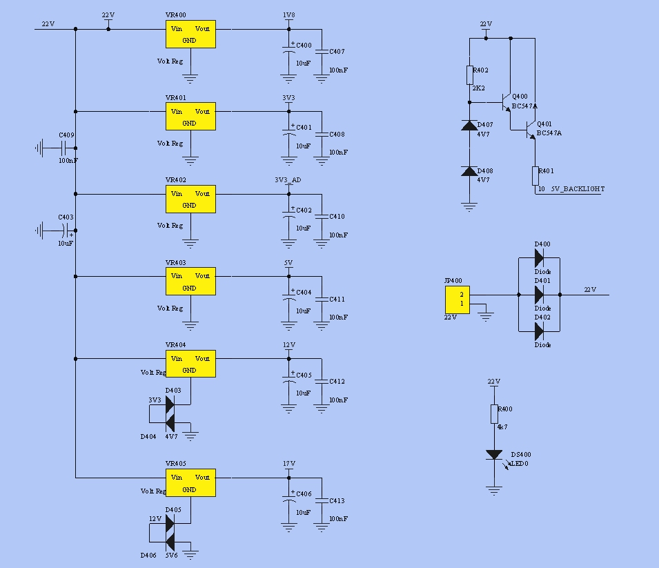
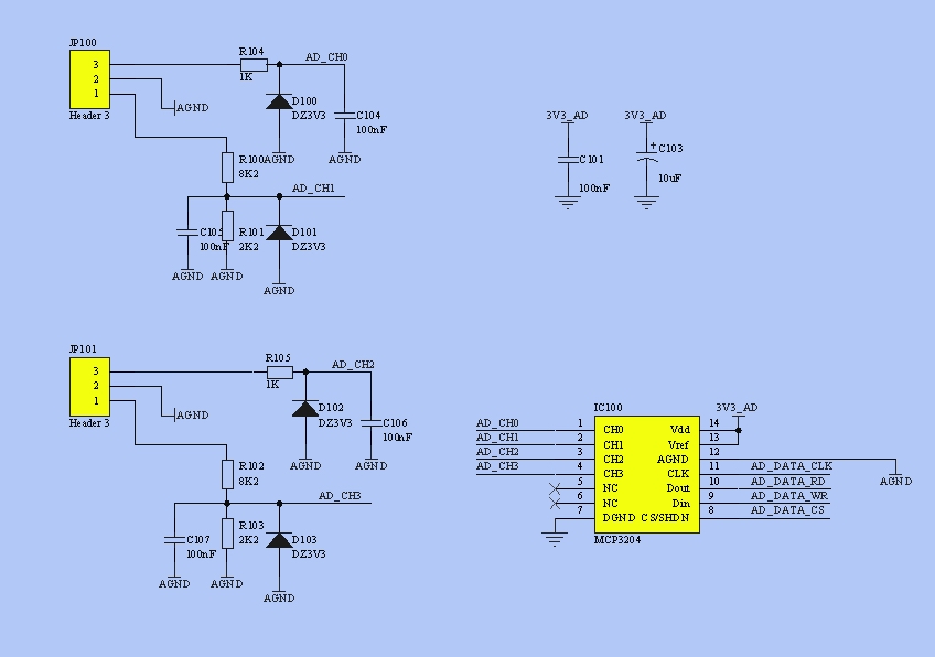
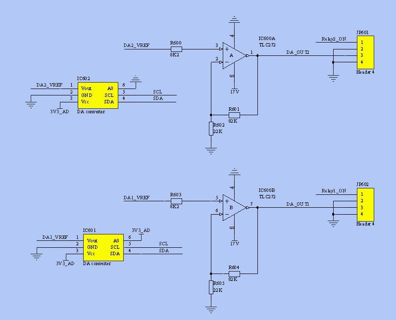
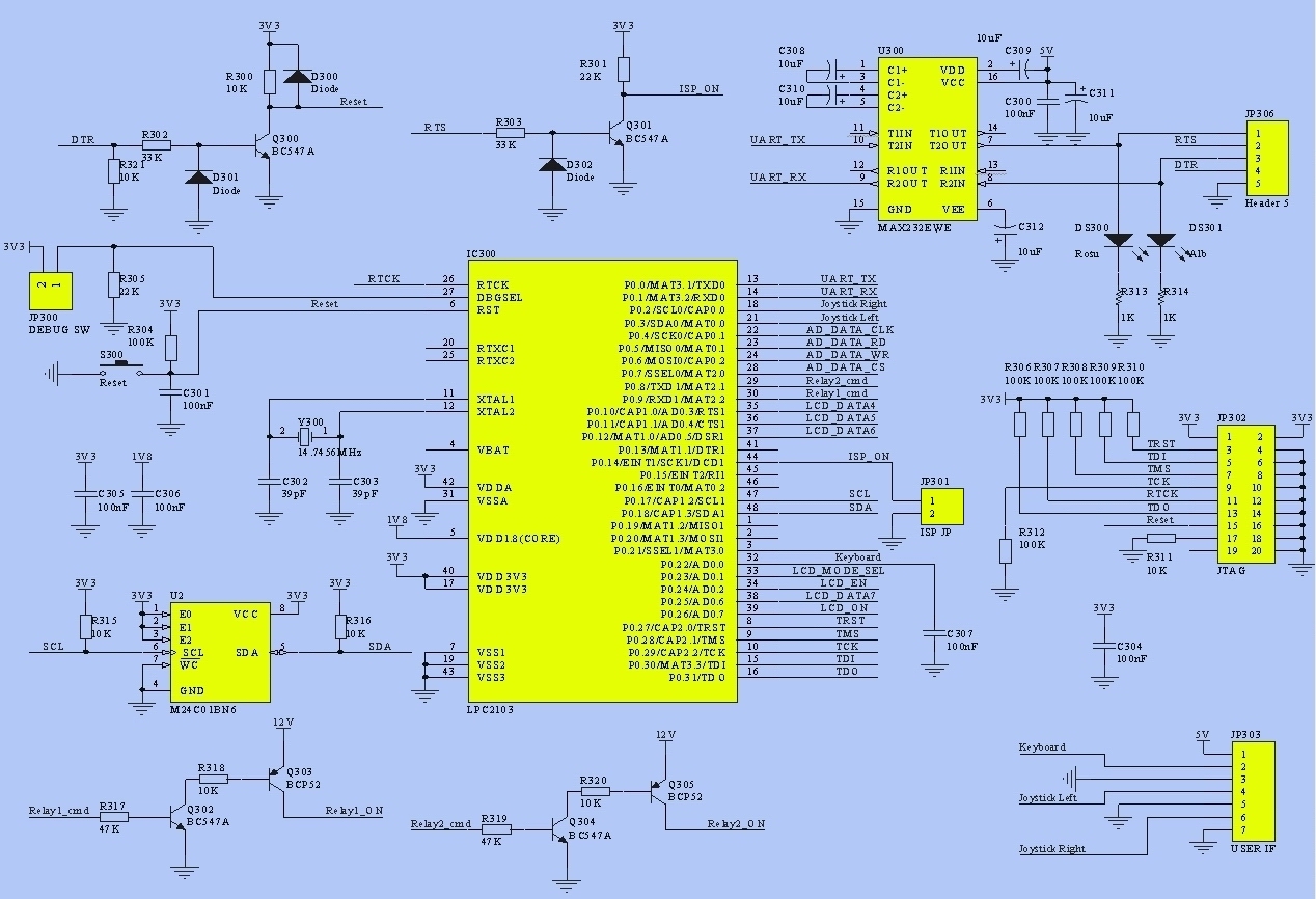
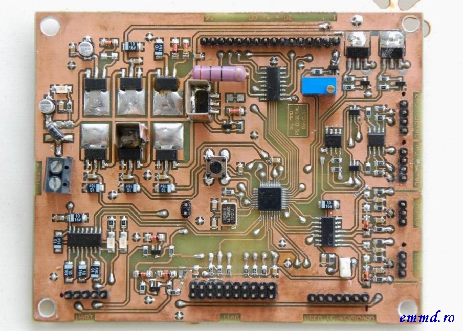
Digital board has 5 blocks: power management, external ADC, LCD interface, DAC and CPU.
Digital board – power management: input voltage: 22-24V. I used 6 regulators, but there are 2 used for 3V3. One is for ADC & DAC blocks, the other one for CPU peripherals and I2C chip. The purpose is to avoid noise on the ADC & DAC line for the measurement stability. There is also one 1V8 output for CPU core, one 5V for UART, keyboard and LCD, one 12V for relays control and one 17V for OP amp supply (12V regulator + some rectifiers). The backlight voltage is not exactly 5V, in fact I tested the LCD first to get a proper backlight, then I modified the supplying circuit.
Digital board – ADC: I used a MCP3204 from Microchip, it is a 4 channels AD converter, controlled over SPI interface: * CH0 : current measurement input for VREG1 * CH1 : voltage measurement input for VREG1 * CH2 : current measurement input for VRE2 * CH3 : voltage measurement input for VREG2 All channels have a zenner rectifier for cutting voltages above 3V3 + one capacitor for noise filtering. CH1 & CH3 have a resistor divider to convert 0…15V to 0…3V3. These resistors should have low tolerance to obtain high accuracy measurements. GND and AGND are different lines here, but will be connected on the VREG board. This is to avoid non wanted electrical effects added by GND plane. In this way the AGND line will have only one route to VREG output.
Digital board – LCD interface: LCD type is LCM2004AWSL. This is an alphanumeric, 4 x 20 characters, which uses the HD44780 controller. A buffer for 3V-5V conversion is placed between CPU and LCD. This controller can run both 8bit and 4bit data interface, hence I used the last one to reduce complexity.
Digital board – DAC interface: MCP4275 is a 12 bit DAC controlled over I2C lines. There are 2, one for each channel. To be able to control the analog modules, I added an OP amplifier in between, to convert 0…3V3 into 0…15V. The OP AMP gain is given by the formula: Vout = Vin*(1 + R604/R605) ~= 4,7.
Digital board – CPU: LPC2103 is a 32-bit ARM7 from NXP. It has 32KB flash + 8KB RAM and it’s driven by an 14,7456MHz Xtal. The storage of preset configurations is located in I2C chip. Debug SW tells the CPU in which mode to boot: normal or debug. I added an UART interface, which makes possible a remote control feature, from PC for example. JP301 is used to control ISP feature, implemented by Q301 & Q302 over RTS & CTS lines. The PCB is dual layer, but all components are placed on the top side.
Few pictures during hardware development:
PCB layouts + components placement in the following links:
- Vreg PCB.
- Vreg components placement.
- User interface PCB.
- User interface components placement.
- Raw voltage source PCB.
- Raw voltage source component placement.
- Front panel.
- Digital part – pcb top.
- Digital part – pcb bottom.
- Digital part – components placement.
For any question please use “Contact form”.
