DIY: Double sided PCB
A full guideline on home made dual layer PCBs.
Although I manage to obtain boards with pretty high level of detail with regards to size and tracks number/width, there are some limitations:
- no solder mask possible, hence no BGA footprint can be used – or yes, but soldering might be difficult and short-circuits prone.
- only 2 layers, top/bottom.
- the vias (electrical joints between same tracks placed on different layers) have to be done manually. During design one has to make sure they are not covered by other components, then once the PCB is ready and drilled, you have to solder small wires between the corresponding pads of the same via – top/bottom.
Notes:
- this procedure can yield tracks of 0,25mm thickness and below.
- the bigger the PCB is, the higher is the probability of mismatch between layers. But, if all below details are followed, one can reach very good results for high sized PCBs.
- To make single layer PCBs the steps related to 2nd layer have to be skipped.
PCB MANUFACTURING STEPS
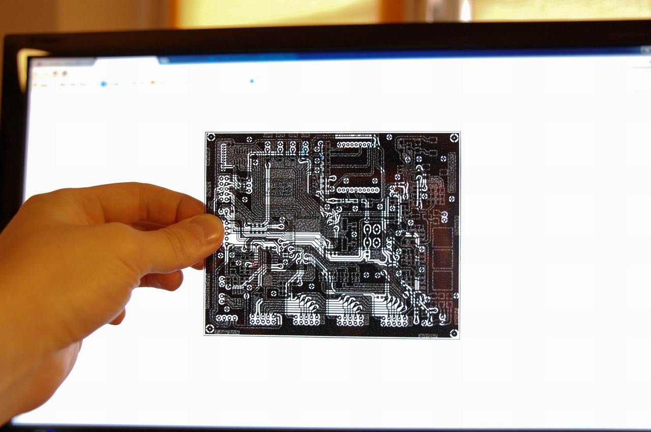
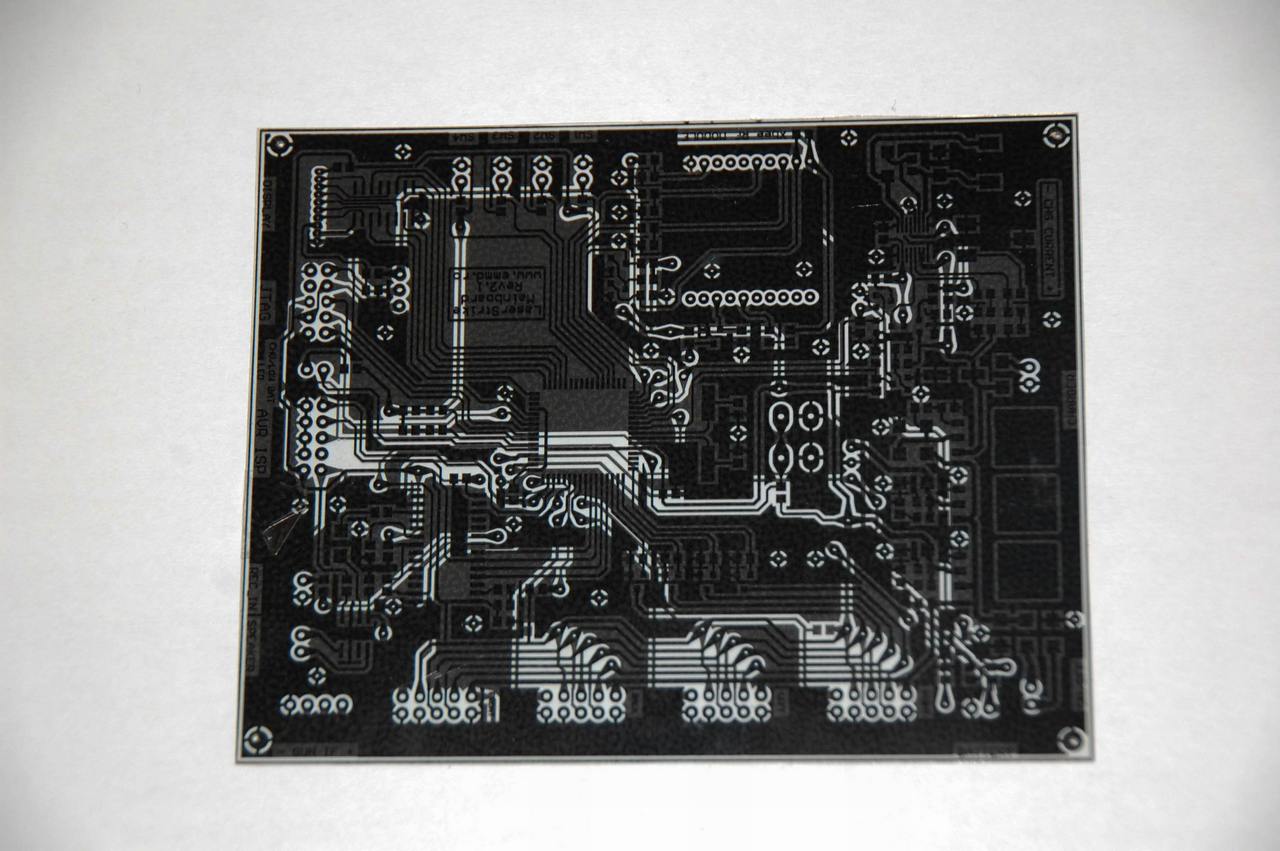
1. PRINTING: you need a laser printer and transparent sheets. Print the top and bottom layers on separate sheets even though they are small in size. Try not to put the fingers on the sheet area before printing 🙂
TIPS:
- transparent sheets must be thicker so that they don’t stretch too much during heating.
- use high resolution > 600 dpi for the printer in order to increase the printing details for small tracks.
- for high areas belonging to the same net (GND for example) the printer will try to optimize the ink so if you place a light under the printed sheet you will notice the inner areas are not so dark compared to the outer areas. This might be an issue during exposure step as the lighter areas will be less “protected”. To adjust this, use a black marker where necessary. Be careful not to step beyond the track edges.
- for 2 layers PCB, do not use the same sheet for printing both layers. Laser printers have to heat the sheet during printing process and this will stretch it. Unfortunately, the sheet will not go back to its original size after printing. Using the same sheet for 2 layers will increase the stretching factor.
- look again at your printed sheet with a light underneath. Laser printer might fail sometimes when it comes for thin tracks, so be prepared with a thin black marker and eventually a lens or a microscope to adjust this.
- try to calculate the hole size for each pad, as printing too small holes will give you troubles during drilling. Drilling should not (as much as possible) touch the copper. Pads/vias are already small areas and drilling might pull them out of the PCB.
- the sheet should be placed (for both top & bottom layers) with the printed side on the PCB. The bottom layer will come like this by default, but top layer should be printed mirrored. This is to ensure no space between the mask and PCB during UV exposure.
- make sure you place (during PCB design) 1 pad in each corner of the PCB (mandatory 3 pads, best 4 pads), with the hole size up to 0.5 mm. These will be used during synchronization step.
- the PCB position has to be such that most of the long tracks will be horizontally placed – when printed as portrait or vertically placed when printed as landscape. This is to ensure the smoothness of tracks, otherwise you might have to adjust more with the marker. The reason behind this is how the printing itself is made. So just rotate the PCB design 90 degrees before printing if needed.
2. TOP/BOTTOM LAYERS SYNCHRONIZATION – SHEETS ONLY: for this step you need additionally some tape. The matching should be initially done with no PCB interleaved, just place the printed layers one on top of the other. The sheets have to be synced, then place some tape to make sure they don’t slip. Place the tape on all 4 edges.
TIPS:
- do the synchronization with a white paper underneath. This will make the pads holes visible and synchronization easier.
- sometimes (usually when the board size is big) you will notice the layers don’t match 100% when placed one on top of the other (seen easy by looking at pads/vias top/bottom) . This is exactly due to the stretching during printing. So you have to print several times until they match.
Sheets synchronization – white background light
Sheets synchronization – white paper underneath
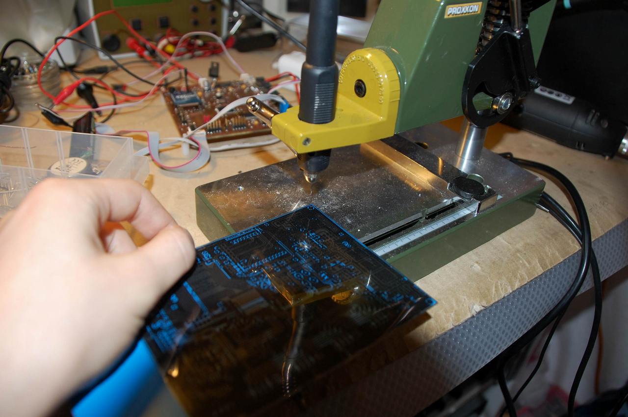
3. PCB-SHEETS SYNCHRONIZATION: a black marker and 4 thin nails are needed. First part of this step consists in syncing the already synced sheets at previous step with the raw PCB. Yes, still not interleaved. This means both 2 sheets (as prepared at previous step) will be placed on top of the PCB. This is just to make the 4 holes corresponding to the 4 pads placed in each PCB corner used for sync. Once you placed the sheets on the PCB, fix them with some tape. Now you have to drill all 4 pads and make sure you do it also through the PCB .
Once this part is done, clean nicely with a brush all the dirt/dust present. Now remove the tape and place the raw PCB between the top/bottom layers. With the nails do the syncing: top sheet – PCB – bottom sheet for all 4 holes. Please note that the nails, drill and pad hole have to match in size. Once the syncing is done, place some tape on all 4 edges for both top & bottom to fix the layers on the PCB. With the black marker make a sign on the board so that you know later on which is the top layer and its position. Now you can remove the nails as the board is ready for UV exposure.
TIPS:
- use high quality raw PCBs. In the past I used to buy a positive spray and do the complete job, but I gave up on this procedure as nowadays you can find already presensitized PCBs which are clearly better than doing them manually.
- if you use presensitized PCBs, make sure you remove the protective sheet only before interleaving the PCB with the 2 printed layers.
- when drilling the 4 pads used for syncing, make sure the drill is perfectly vertical. A small angle means different positions for the pad hole with regards to the top/bottom sides. This in turn means synchronization failure, or high error. If needed, use a support for the drilling machine as shown in the picture below.
- don’t forget to mark the top layer on the PCB (with the marker) otherwise the syncing will fail.
- if the board used is bigger than your PCB design, do NOT cut it before finishing the PCB (all steps here). The reason behind this is the fact that cutting the PCB might bend it and this will affect the UV exposure.
Sheets – PCB sync: drill 4 sync holes
Sheets – PCB sync #1
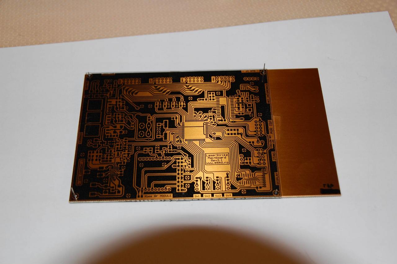
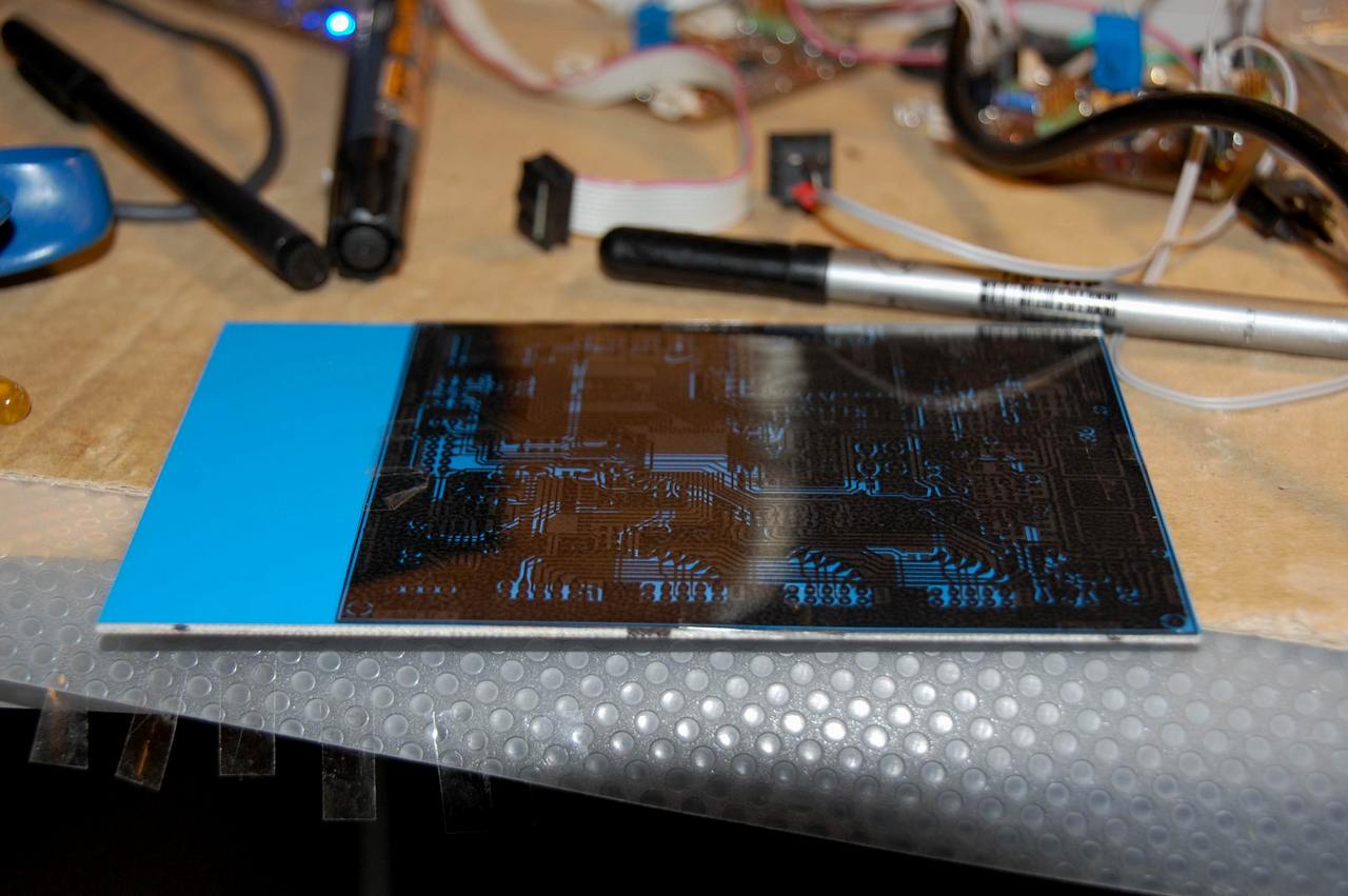
Sheets-PCB top/bottom synced, ready for UV exposure
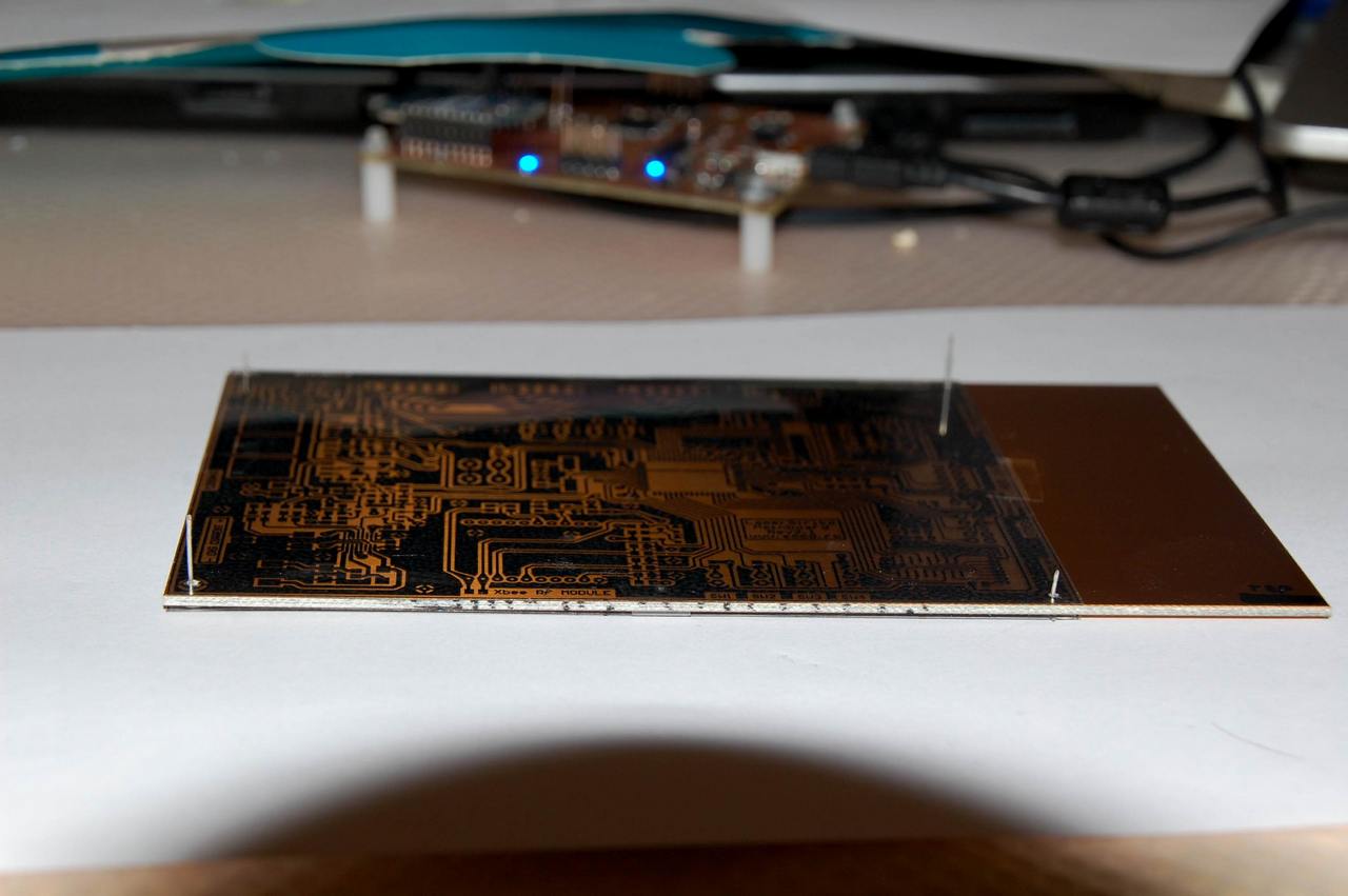
Sheets-PCB top/bottom synced, ready for UV exposure
4. UV EXPOSURE: now you need an UV lamp. This is tricky as different lamp models produce different UV power levels, resulting in different exposure times. In the past I used a self made lamp, but later on I bought one which I still have and it’s excellent. Depending on the lamp you have to go for the trial method until you reach the best time for your setup.
TIPS:
- regardless of the used lamp, make sure the exposed side has no space between the sheet and PCB. This is to avoid UV light hitting the masked parts. For this you may use 2 pieces of glass (sandwich method), place the PCB in between and fix this system with something so that the PCB doesn’t slip out of it. If you use a professional lamp it should take care of this part for you.
- do some PCBs for testing the UV exposure time beforehand. Different types of presensitized boards require different exposure times. Short exposure time means non masked part is not completely “destroyed”, whereas long exposure time means possible damage of the masked part (masking is not perfect => small UV light will still go through your mask).
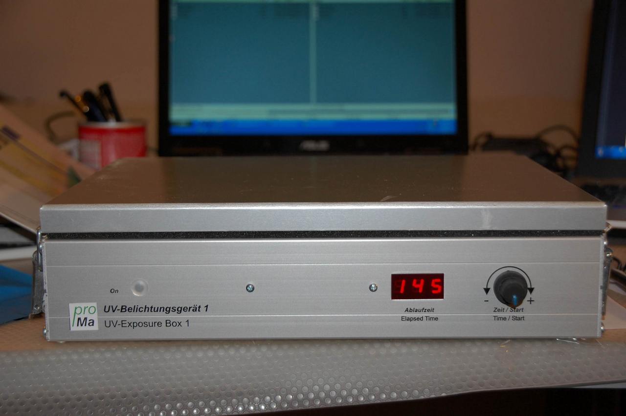
Professional UV lamp
5. PCB DEVELOPMENT: this is another step where trial method should be applied for preparing the developer (unless you buy it already prepared). What I observed is that violet positive requires 4,2 grams of sodium-hydroxide whereas presensitized PCBs that I use require 1,2-1,3 grams. Both quantities are expressed for 400ml water. It should take app. 3-5 minutes until the non masked part is removed. It should look like in the below pictures.
TIPS:
- keep the tub still until the process is finished.
- once done, use a soft brush to parse gently both top & bottom areas so that you remove any remaining particles.
- the process should be visible in the first minute. If nothing happens within 1-1,5 minute, your mixture is not efficient, so you should redo it with a higher concentration of hydroxide.
- as soon as you finished with the brush, wash it and dry it: keep it 5-10 minutes in a vertical position.
- make a visual check whether everything looks OK. You might see tracks damaged or unified, so take several minutes to inspect the board at this step to avoid further troubles. Use the necessary tools to adjust the above issues (like marker, a thin tweezers).
PCB developed, ready for etching
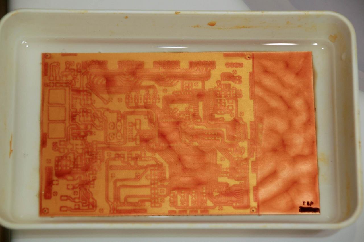
PCB during development
6. ETCHING: now you have to remove all non masked copper and you’re good to go. Either you make or you buy this substance: ferric chloride. If you buy it it’s easier, although costs more money, if you make it yourself, again you have to do some experiments to reach small etching times. Please remember, with each PCB you make this substance will become lighter and corrosion time will increase. In short, what you do now is to place the substance and the PCB in a tub and leave them till etching it’s done. When ready, wash it and remove the mask using acetone.
If everything went OK, you can drill your PCB and start mounting components.
TIPS:
- hang something on the board so that you can easily take it out from the tub. Best to use is the fishing line, it cannot be damaged by this substance. (do not place metal wires!!!)
- best tip here is related to the shortening of etching time. You can manufacture something for that, like I did. That’s an aquarium pump which pushes air on the bottom of the tub. With the board placed vertically, the pushed air will whirl the substance and hence speed up the process.
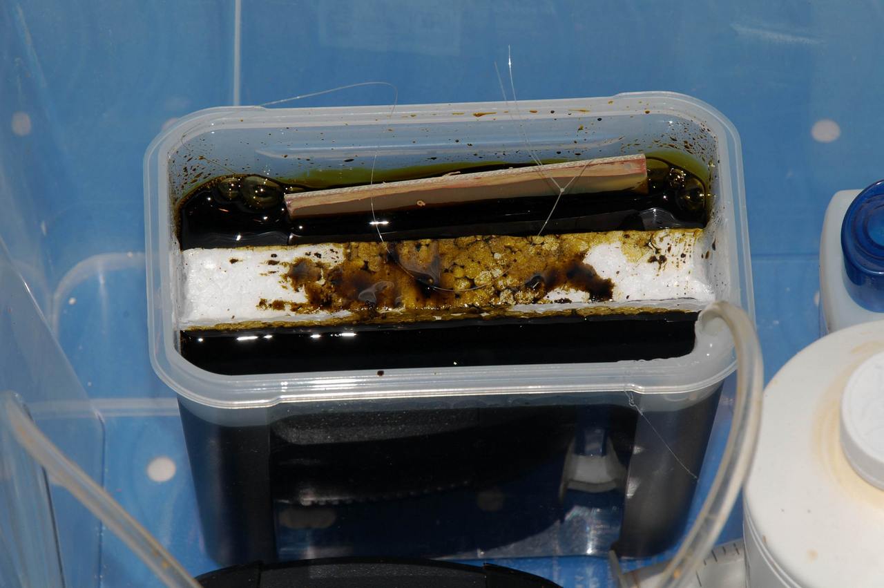
Enhanced etching tub
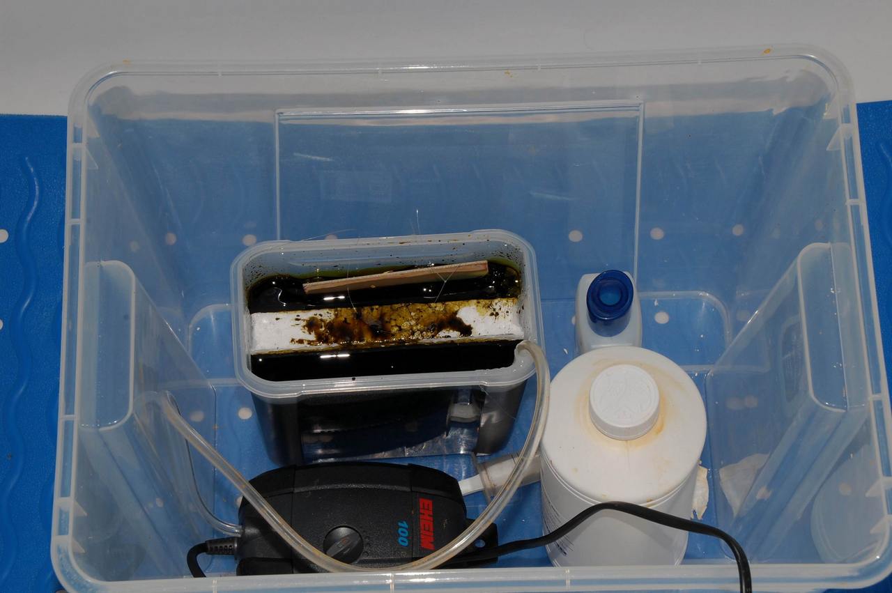
Enhanced etching tub
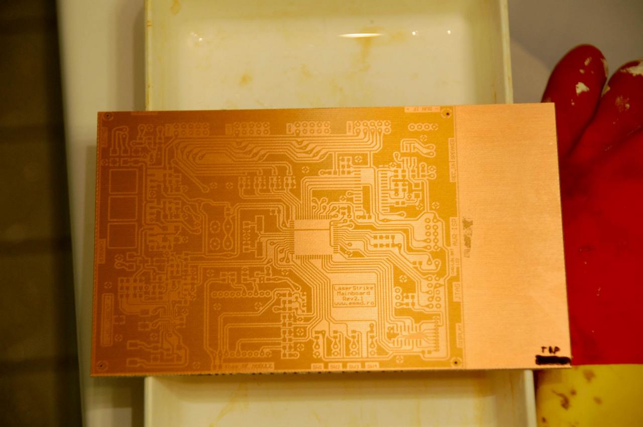
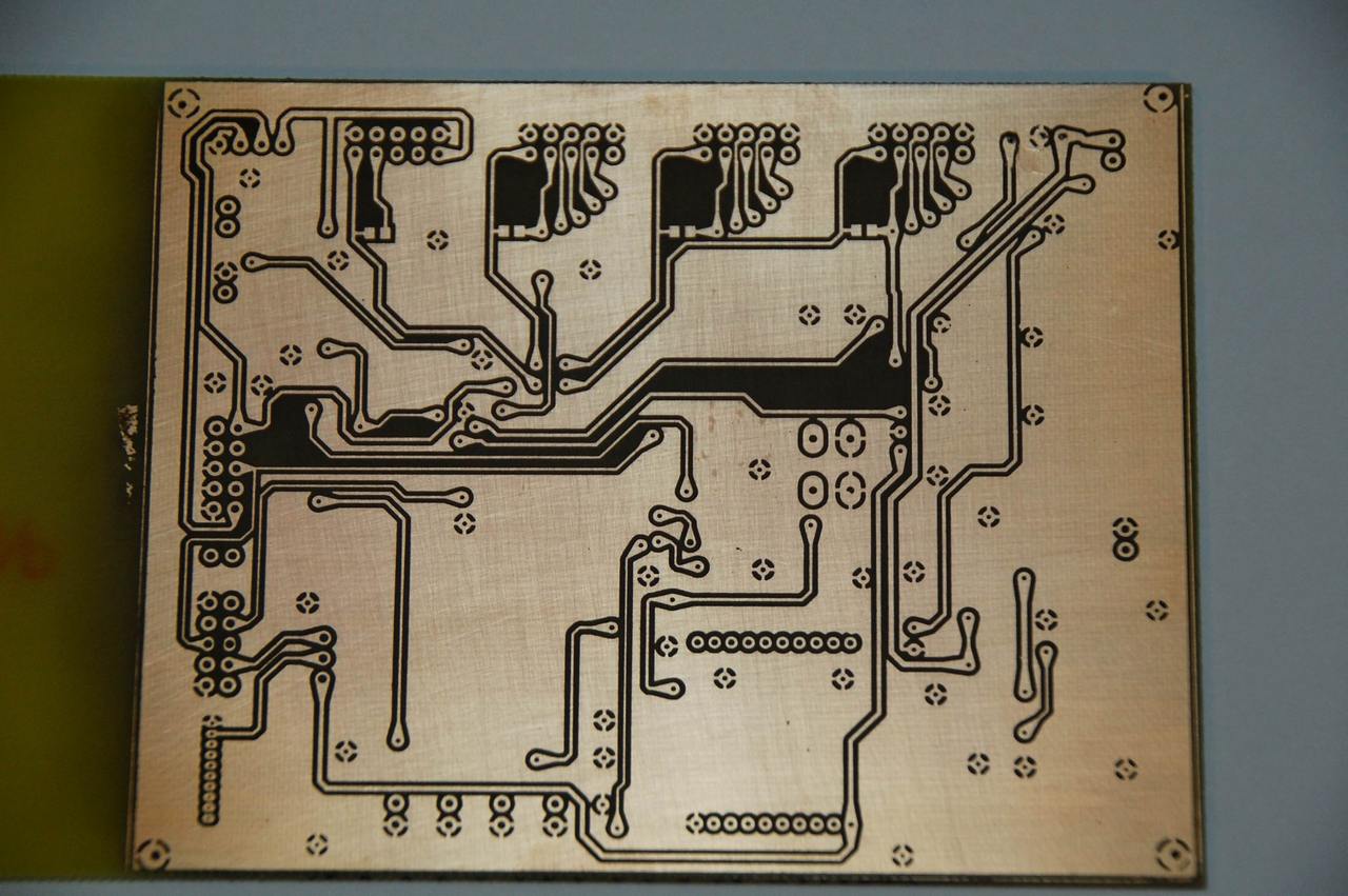
That’s all, now we have our pcb ready for components placing. Have a look below at the outcome. Do not forget to link the vias between the 2 layers.
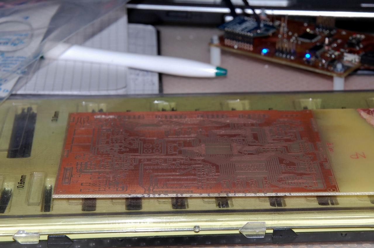
PCB ready – not yet cut
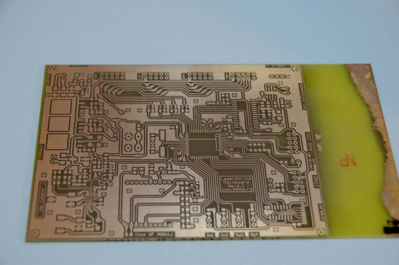
PCB ready – not yet cut
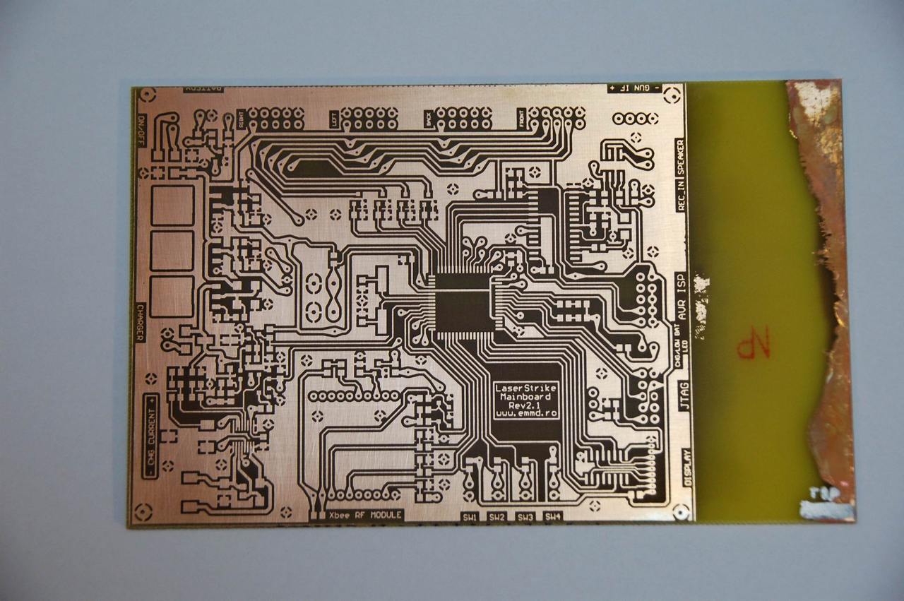
PCB ready – not yet cut
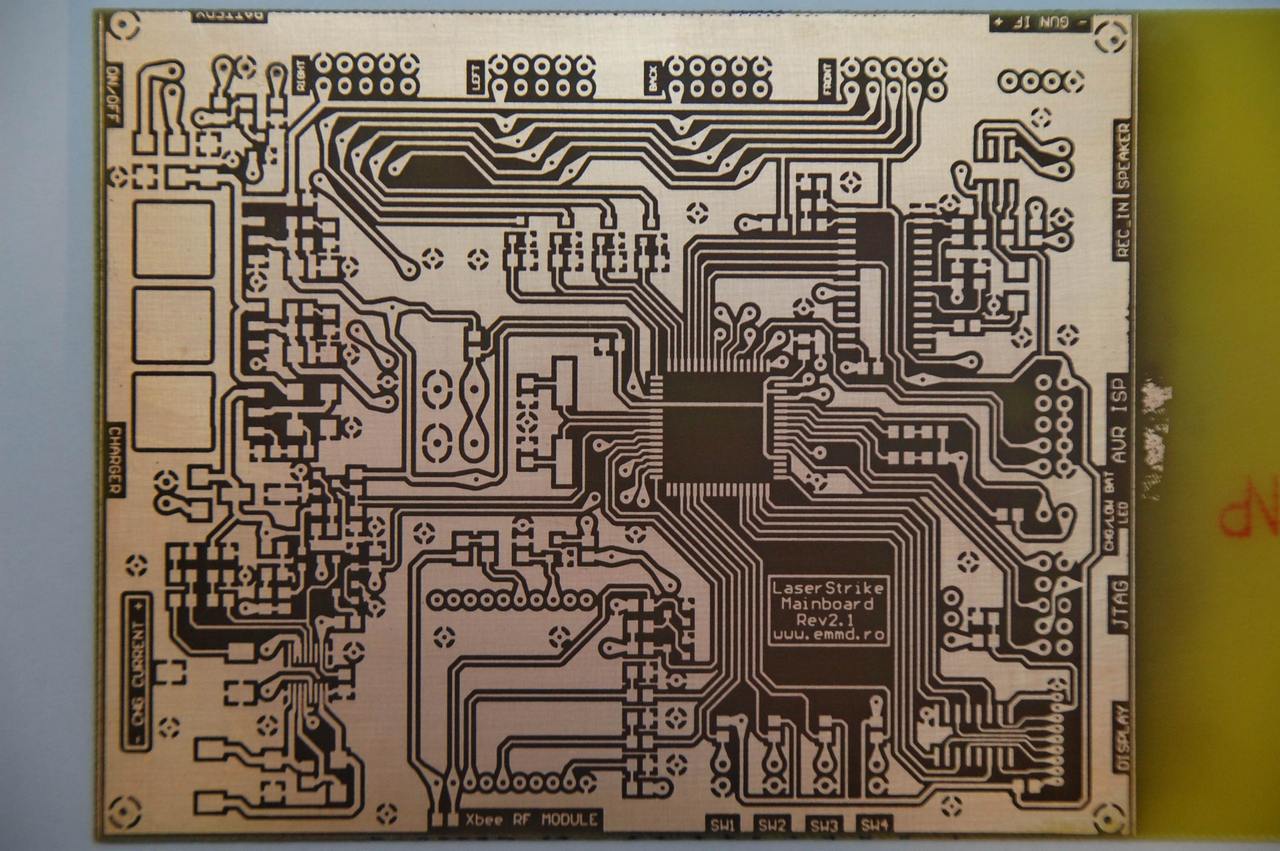
PCB ready – not yet cut
PCB ready – not yet cut
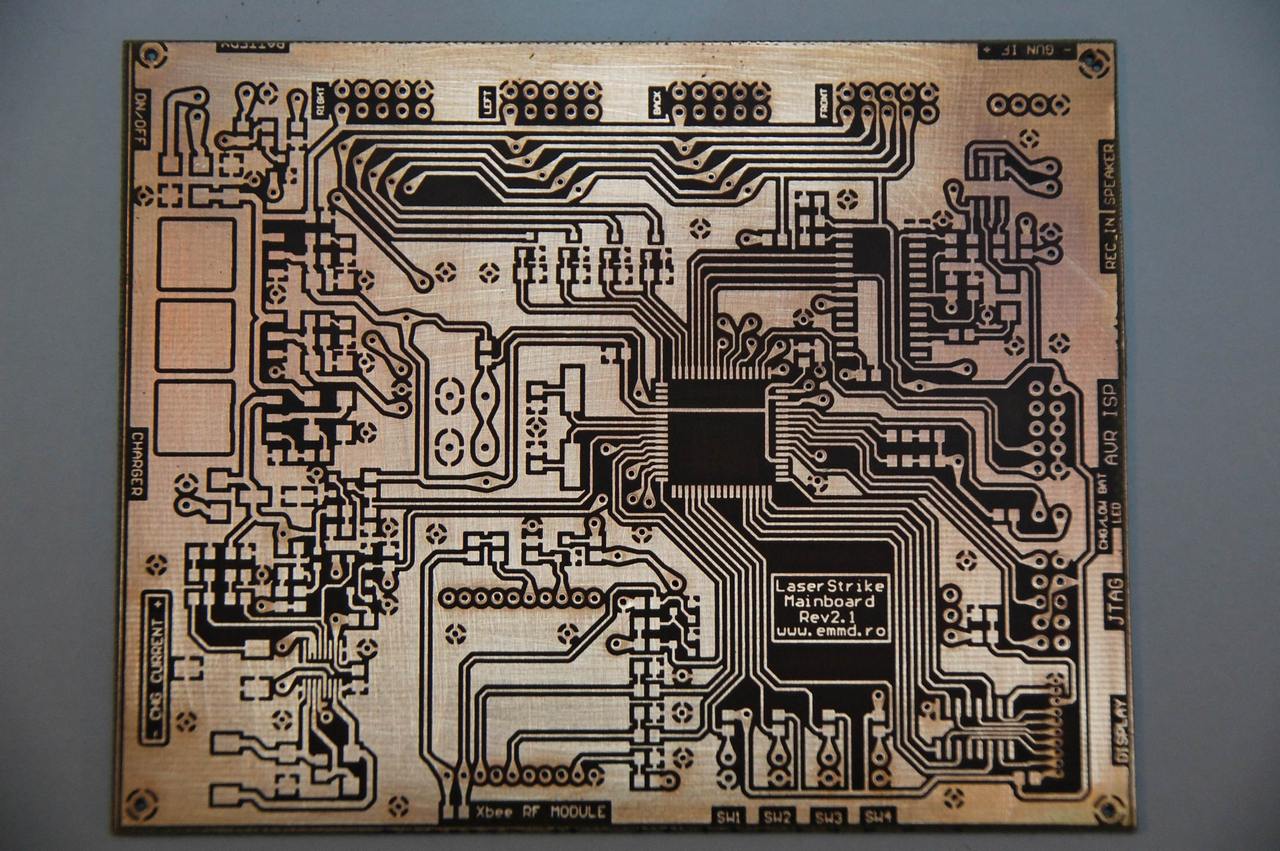
PCB ready
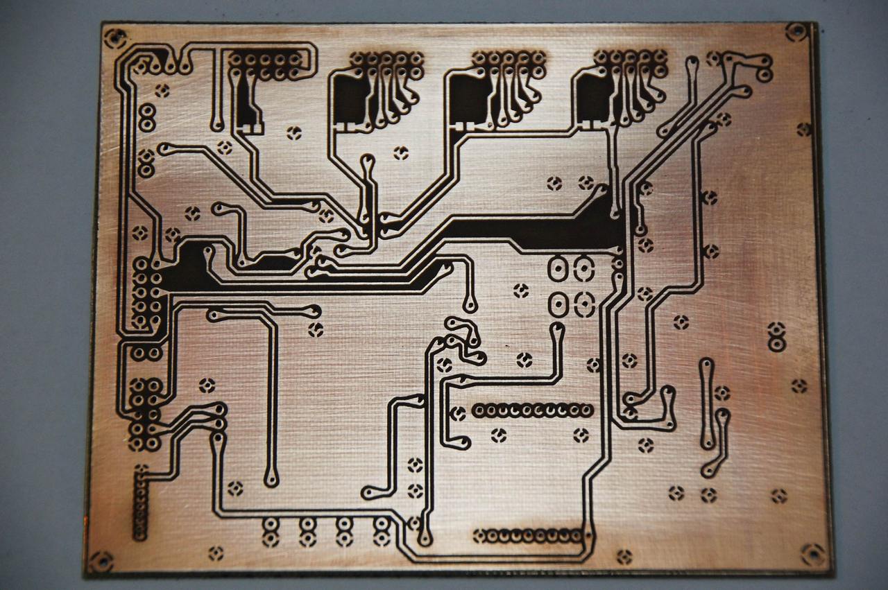
PCB ready – bottom layer
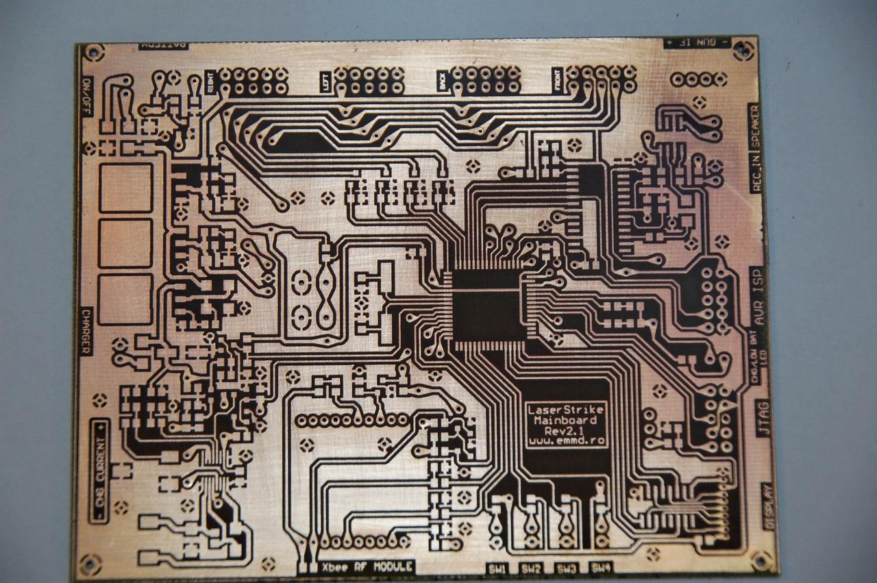
PCB ready – top layer
Note: please be aware that this process uses chemical substances which are dangerous, so make sure you do it in a safe vented area with the appropriate gloves/masks.
For any comments/questions please use “Contact” form.