Vag Com 4.02 USB interface
A couple of years ago I was looking for a vag com interface for my car. Found 2 solutions: 1-buy one; 2-make one. Buying one was relatively cheep but I decided to build one although I knew the KKL transceivers are not easy to find. Anyway, after purchasing some of them, enough to make 3 or 4 interfaces I started building the cable.
This version is suitable for VAG group (Volkswagen, Skoda, Seat & Audi) up to 2004, although I found 2004 cars not being able to establish KKL communication for all modules. The engine was always reachable but e.g. comfort module (#46) was giving communication error on some cars.
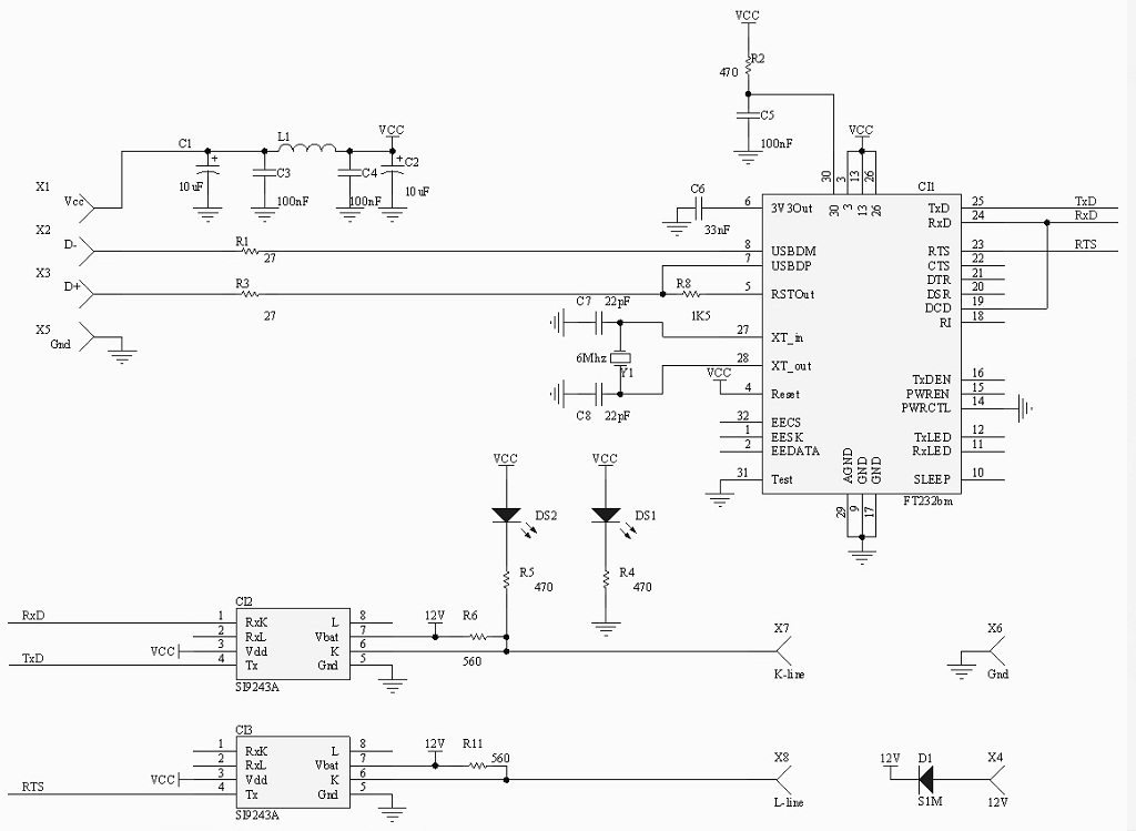
VAG COM 4.02 schematic
Quick overview on the schematic: there are 3 control lines (KKL), visible also between input and output stage: TxD, RxD, RTS. Output stage is the fixed one, around SI9243 transceivers; input stage can vary between RS232 and USB communication. In this article you’ll find the USB part. Input stage can be taken from FTDI (FT232) datasheet. There are 2 LEDs, DS1 will show 12V available on OBD side, DS2 will start toggling once data is exchanged. Other details: D1 can be almost any type, here is a typical S1M(1A) rectifier. I didn’t place any inductor (L1) as I didn’t have it at that time, just replaced it with a simple wire.
The layout is made to fit in an OBD connector medium sized. Best case for the PCB is to be dual layer to use the bottom one as GND plane. I used single layer so I had to link all GND vias underneath. PCB layout can be downloaded from here. It is mirrored so it should be placed with the printed part on the PCB. This is to have no space between mask and PCB during UV exposure.
Here below the components layout and one shot with the board assembled.
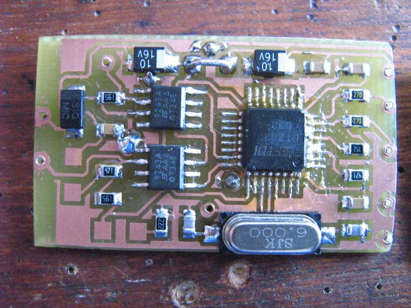
Vag Com board assembled
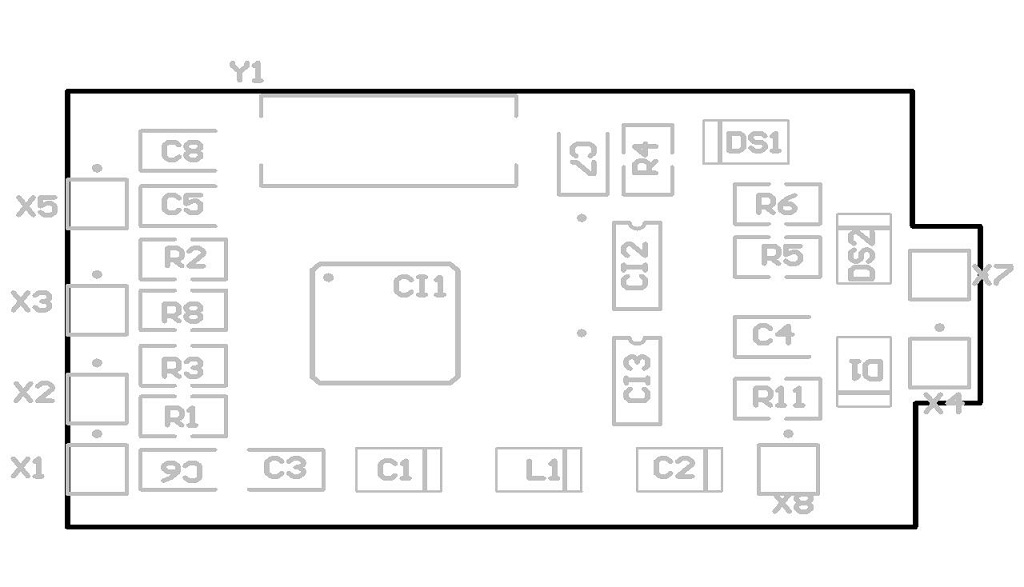
Components placement
The 2 LEDs are placed on the top side of OBD connector to be visible. As cable I used one from a defect mouse. On the input stage, the GND and VCC of USB cable can be quickly spotted (with a multimeter for example), the USB+ and USB- can vary depending on wire colors. Better check USB pinout or try inverting the order if it doesn’t work.
The connection between output stage and OBD connector can be seen below. For the OBD: pin 4 = GND; pin16 = VBAT; pin7 = K-line; pin15=L-line.

Overview on bottom side
Overview on board – OBD connection
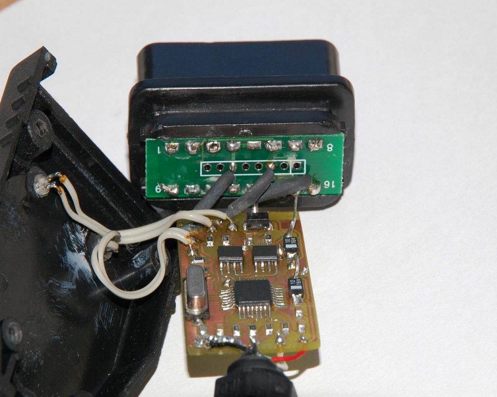
Finally, this is the assembled cable. It doesn’t need any calibration or adjusting as it doesn’t contain any firmware. It should work straight forward.

Final interface cable
Please be aware that this is notoy, it should be used only by those who know what vag-com means. I will not be liable for any damage arising directly or indirectly from building/using vag-com cables as described on this page.
Again the link for the PCB: pcb_link.
For any question please use “Contact form”.